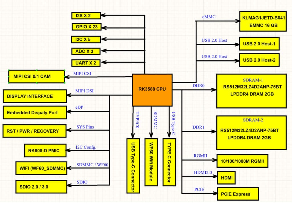
Introduction
Many designers find it challenging to organize their schematics when working on complex electronic designs. A poorly arranged schematic can lead to errors, longer debugging times, and communication issues within teams. Imagine designing an advanced IoT device with multiple subsystems—power management, wireless communication, sensors, and microcontrollers—all intertwined in a single schematic. Without proper structure, the task becomes daunting, prone to confusion and mistakes. This is where modular design techniques come to the rescue. By breaking down complex circuits into manageable modules, designers can create schematics that are not only easier to understand but also scalable and reusable.
In this article, we will explore the principles, steps, and best practices for applying modular design techniques to schematic circuits, ensuring clarity, efficiency, and error reduction in your projects.
Why Modular Design is Crucial for Complex Boards
Modern electronic systems are often composed of multiple interconnected subsystems, each performing a specific function. Attempting to capture all these subsystems in a single, flat schematic can quickly become overwhelming. Modular design addresses these challenges by:
- Improving Clarity: Dividing the circuit into smaller, functional blocks makes it easier to visualize the overall design and understand individual sections.
- Simplifying Debugging: With well-defined modules, faults can be isolated to specific sections, reducing troubleshooting time.
- Enhancing Scalability: Modular designs allow for easier expansion. For instance, adding a new feature might only require creating and integrating a new module without overhauling the entire schematic.
- 4. Facilitating Reusability: Modules can be reused in future projects, saving design time and effort.
For example, consider a complex drone design. By breaking it into modules like power distribution, motor control, communication, and sensors, each team member can focus on their section, resulting in a faster and more reliable design process.
Steps to Implement Modular Design in Schematic Circuits
1. Break Down the System
The first step in modular design is identifying the key functional blocks of your circuit. Ask yourself:
– What are the core functionalities of the design?
– Which parts of the circuit can operate independently?
For example, in a home automation system, the functional blocks might include:
– Power supply
– Microcontroller unit (MCU)
– Wireless communication module (e.g., Wi-Fi or Zigbee)
– Sensor interface
– Actuator control
2. Design Each Module Independently
Once the system is divided into modules, focus on designing each block independently. This involves:
– Choosing the appropriate components for the module’s function.
– Ensuring the internal connections within the module are complete and error-free.
For example, in a power supply module, include all necessary components such as voltage regulators, decoupling capacitors, and protection circuits. Test this module in isolation before integration.
3. Define Clear Interfaces
Each module must have clearly defined input and output interfaces. These interfaces are the connection points between modules, such as power lines, signal buses, or control lines.
To define interfaces:
– Label all pins and connectors with meaningful names (e.g., “VCC_5V”, “UART_TX”).
– Ensure that signals crossing module boundaries adhere to agreed-upon standards (e.g., voltage levels, protocols).
4. Integrate Modules
With all modules designed and interfaces defined, the next step is integration. Place the modules together in the main schematic, connecting their interfaces as per the overall design requirements.
During integration:
– Use consistent labeling to avoid confusion.
– Double-check connections to ensure compatibility between modules.
For instance, ensure that the I2C communication lines from the sensor module connect properly to the MCU module without swapping SDA and SCL.
Best Practices for Modular Schematic Design
1. Use Hierarchical Design
Hierarchical design involves organizing your schematic into separate sheets, each representing a module. Most schematic capture tools (e.g., Altium, KiCAD) support hierarchical design through features like sheet symbols and sub-sheets.
Benefits of hierarchical design include:
– Simplified navigation within the schematic.
– Clear visualization of module boundaries and interconnections.
– Easier documentation and review processes.
2. Maintain Consistent Naming Conventions
Adopt a consistent naming convention for designators, nets, and symbols. For example:
– Use prefixes to indicate module association (e.g., “PWR_VCC” for power supply nets, “MCU_UART_TX” for MCU signals).
– Avoid generic names like “NET1” or “SIGNAL_A”, as they can lead to confusion.
3. Document Each Module
Accompany each module with detailed documentation, including:
– A brief description of its function.
– Input/output specifications.
– A list of components with part numbers.
4. Plan for Testing
Design with testing in mind. Include test points and diagnostic indicators (e.g., LEDs for power and signal activity). Testing each module independently before integration ensures that errors are caught early.
Case Study: Modular Design for a Smart Home Controller
To illustrate the modular design process, let’s consider a smart home controller with the following requirements:
– A power supply that converts mains power to 5V and 3.3V.
– An ESP32 microcontroller for processing and communication.
– Temperature and humidity sensors for monitoring.
– Relay controls for switching home appliances.
Modular Breakdown:
1. Power Supply Module: Includes a 5V buck converter, a 3.3V LDO regulator, and decoupling capacitors.
2. Microcontroller Module: Houses the ESP32, crystal oscillator, and essential GPIO headers.
3. Sensor Module: Interfaces the DHT22 temperature and humidity sensor with necessary pull-up resistors.
4. Relay Module: Contains relays, optocouplers, and driver circuits for controlling high-power devices.
Each module is designed and tested independently. The power supply is verified for stable voltage outputs. The sensor module is checked for accurate data readings. Once all modules are validated, they are integrated into the main schematic, ensuring proper connections and signal compatibility.
Conclusion
Modular design techniques are essential for managing the complexity of modern electronic circuits. By breaking a system into functional modules, defining clear interfaces, and following best practices, designers can create schematics that are organized, scalable, and easy to debug. Adopting modular design principles will enhance the efficiency and reliability of your projects.
