Introduction
The electronic industry faces an increasing demand for an efficient and effective product development process to introduce new products to the market. To stay competitive, these products must be innovative, feature-rich, reliable, and cost-effective. However, the current development process has its challenges. From the outset, once the new product’s functionality has been determined, electronic schematic designers (also known as Hardware developers/designers) face a lack of automated tools for verifying the integrity of their schematic designs. Consequently, they must manually analyze each component meticulously to ensure it aligns with the instructions provided in the components manufacturers’ datasheets. Moreover, ensuring compliance with specific industry requirements, especially in sectors like Aerospace or Automotive, poses even greater challenges. Additionally, confirming that the components can be procured within an acceptable time frame and are not reaching their end-of-line stage adds further complexity to the process.
Electric circuits serve as the foundation for every modern electrical device. In recent decades, as the physical size of electrical components decreased (exemplified by “Moore’s law”) and functional demands have risen significantly, the complexity of circuit designs has drastically increased. This arises from the need to accommodate a higher number of components constrained by limited real estate. These components encompass simple passive elements like resistors, capacitors, inductors, diodes, as well as sophisticated active components like microprocessors, FPGAs, voltage regulators, sensors, and more.
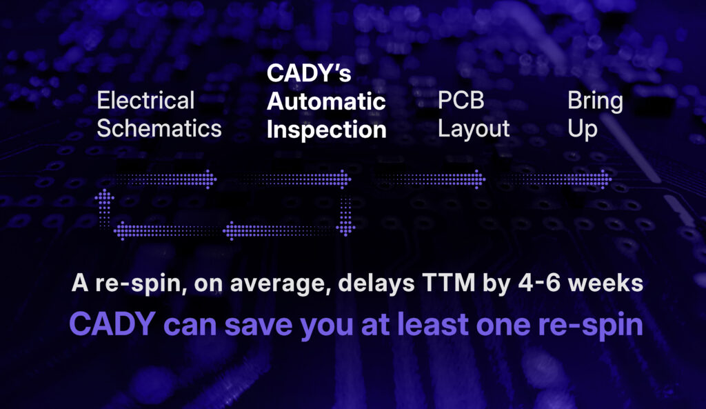
When developing a new electronic product, the typical process involves designing the electrical schematic using an ECAD (Electronic Computer-Aided Design) system, followed by a schematic design review upon completion. The design then moves on for layout roughing, leading to the manufacturing and assembly of a printed circuit board (PCB) for the initial “Bring-Up.” During this phase, the envisioned electronic circuit is physically realized and tested using laboratory equipment and other physical testing methods. However, the combination of increased functionality demands, and limited real estate has made schematic designs highly complex and extremely challenging to create and debug within a reasonable timeframe. Consequently, achieving an error-free design on the first iteration has become nearly impossible.
Currently, a significant portion of the schematic design review relies on designers manually reading electric components’ datasheets to verify that each component meets the required specifications, and that the design’s functionality aligns with the desired requirements. Unfortunately, errors often go unnoticed, ranging from simple wrong connections to complex logical errors, preventing the circuit from performing as intended. When errors are detected, the schematic and layout must be corrected accordingly, resulting in a “re-spin” of the design. These re-spins are costly, time-consuming, and wasteful, and they frequently delay the product’s market launch.
In some cases, design errors may remain hidden until the product is already on the market. This can result in product recalls, on-site repairs, damage to the company’s reputation, and substantial financial expenses. Evidently, a need exists for an automated system that can detect errors during the early stages of the process. Such a system would help decrease the number of project re-spins and greatly reduce the risk of defective products reaching the market.
The Solution
Existing Electrical Schematics Review Tools
Several techniques are available for reviewing and validating PCB designs, encompassing functional analysis, timing simulations, and logical equivalence checking, where the new circuit model is compared to a reference model representing the desired functionality. Although these techniques prove valuable, they may not sufficiently identify errors or suboptimal designs related to datasheet information, such as missing pull-up/down resistors, communication protocol line mismatches, exceeding operating conditions (voltage, current, temperature, etc.), violating direct connection instructions, incorrect component placements, and traces routing issues, among others. While verification software tools like “Design Rules Check” (DRC), such as “Valydate Schematic Analysis” in Mentor Graphics’ Xpedition package, can partially detect some of these errors, they have limited capabilities in detecting design errors across a broader spectrum. They lack the ability to access, process, understand, and implement datasheet information effectively. Consequently, the electronic industry still heavily relies on manual design reviews, a slow, cumbersome, and error-prone process, leading to repetitive design iterations or “re-spins.”
As a result, the electronic industry is in dire need of an automatic electrical circuit design analysis system. This system should possess the ability to detect a wide range of errors, incorporate best-practice guidelines, and provide simultaneous bottom-up and top-down perspectives. It should be capable of verifying specific component requirements while aligning them with the overall design requirements.
CADY’s System Methodology
CADY developed a solution that effectively addresses the industry’s needs and resolves the problem at hand. The system’s functionality revolves around scanning electrical component datasheets and extracting pertinent information related to the schematic design. Below is a summary of the process: The process commences by scanning the datasheets and analyzing the information relevant to the schematic design. It then extracts the desired information item (for example, a pin’s voltage range). The extracted information is further processed using specialized NLP (Natural Language Processing) and image processing algorithms to infer the requirement or property it represents.