Introduction
In electronics design, schematics serve as the backbone of any project, acting as a detailed map that guides engineers. They are crucial for conveying design intent, functionality, and component interconnections. However, even the most well-designed schematic can be rendered ineffective if it lacks clear annotation and labeling. This article delves into why annotation and labeling are important for effective schematic design and how they contribute to successful project execution.
What is Annotation and Labeling in Schematics
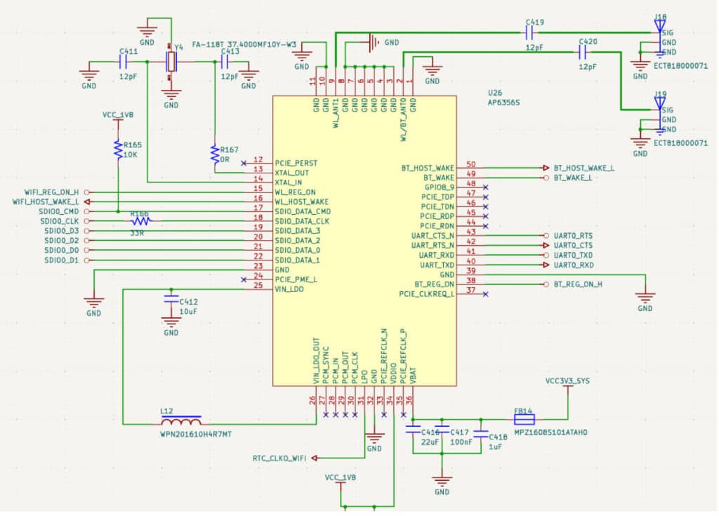
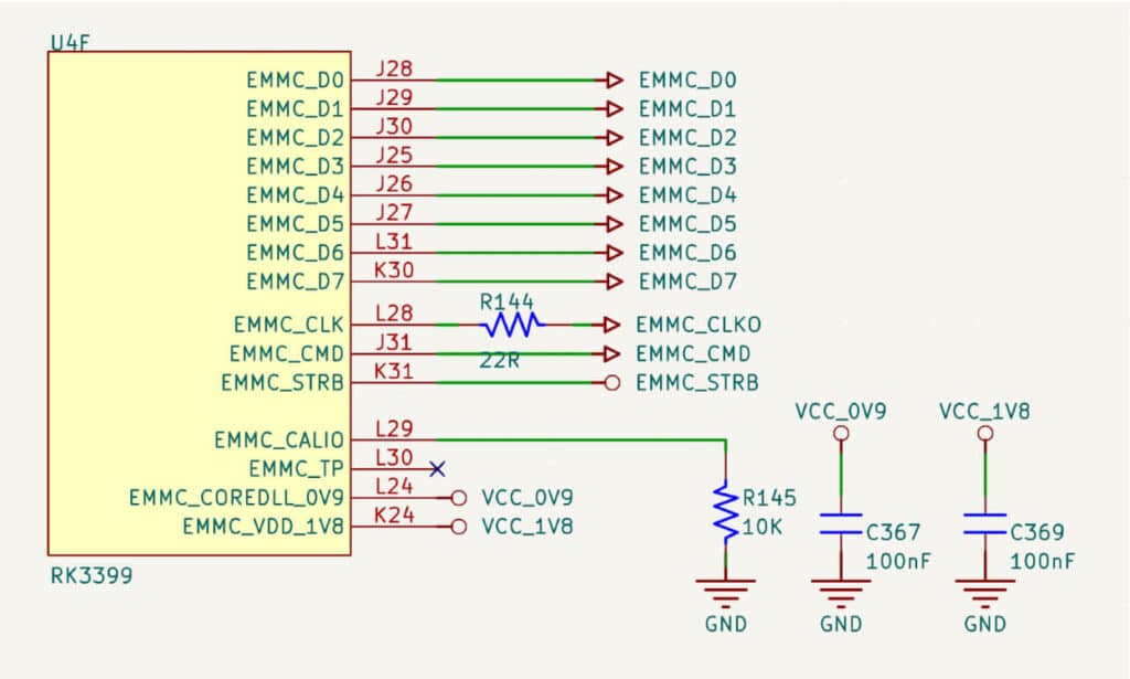
Annotation and labeling refer to the practice of adding descriptive information and identifiers to various elements within a schematic. Annotations typically include textual details such as component values, tolerances, and specifications, while labels often consist of identifiers like reference designators (e.g., R1, C2, U3) and net names (e.g., VCC, GND). Together, they provide context, making the schematic more readable and easier to understand.
Benefits of Proper Annotation and Labeling
Enhanced Clarity and Readability
One of the primary benefits of proper annotation and labeling is the enhanced clarity they bring to a schematic. A well-annotated schematic allows anyone who reads it, be it a fellow engineer, a technician, or a manufacturer to quickly grasp the circuit’s functionality and interconnections. This clarity is particularly vital in complex designs where a single page can contain numerous components and connections.
Improved Debugging and Troubleshooting
Clear annotation and labeling are invaluable when it comes to debugging and troubleshooting. Imagine a situation where a circuit is not functioning as expected. A well-labeled schematic enables the engineer to quickly identify and locate components, trace signal paths, and isolate potential issues. Conversely, a poorly annotated schematic can lead to confusion, misidentification of components, and increased time spent on troubleshooting. This can be especially problematic in time-sensitive projects or when issues arise during field deployments.
Streamlined Communication and Documentation
Schematic annotations serve as a universal language in electronics design. They help in effectively communicating the design intent across various teams involved in a project, including design engineers, PCB layout designers, and manufacturing teams. Well-documented schematics with clear labels reduce the chances of miscommunication, ensuring that each team has a precise understanding of the design. This is particularly important in collaborative environments or when transitioning a design from one team to another.
Types of Annotation and Labeling
Reference Designators
Reference designators are unique identifiers assigned to each component in a schematic, such as R1 for a resistor, C2 for a capacitor, and U3 for an integrated circuit. They provide a straightforward way to reference components during discussions, debugging, and documentation. Proper use of reference designators ensures that every component is easily identifiable, reducing the risk of confusion or mistakes during assembly and testing.
Component Values and Specifications
Annotations such as resistor values, capacitor ratings, voltage tolerances, and IC part numbers provide critical information for both design and assembly. Including these details directly on the schematic eliminates the need to cross-reference other documents and ensures that the correct components are used. This is particularly important in preventing assembly errors and ensuring that the circuit performs as intended.
Net Labels
Net labels are used to identify electrical connections between different points in the circuit, such as VCC, GND, or signal names like DATA. They simplify the schematic by eliminating the need for extensive wiring diagrams and make it clear how different parts of the circuit are connected. Net labels also help in understanding the signal flow and in verifying that the intended electrical connections are correctly implemented.
Cross-Referencing
For designs that span multiple schematic sheets, cross-referencing is essential. It involves using markers or labels to indicate where a signal or component continues on another sheet. This practice helps trace connections and signal flows across different parts of the schematic, providing a cohesive view of the entire design.
Best Practices for Annotation and Labeling
- Consistency: Maintaining consistency in naming conventions, abbreviations, and annotation styles throughout the schematic is important. Inconsistent labeling can lead to confusion and misinterpretation, especially in collaborative projects. Establishing a clear set of guidelines for annotation and ensuring adherence to them can greatly enhance the schematic’s readability and professionalism.
- Clarity Over Density: While it’s important to provide enough information, over-annotating a schematic can clutter it and make it difficult to read. Aim for clarity by using concise labels and only including necessary details. Consider the balance between providing enough information for understanding and avoiding visual overload.
- Use of Standards: Adhering to industry standards such as IEEE or IPC standards for schematic annotation ensures that your designs are compatible with industry norms and expectations. Standards provide a common framework for annotation and labeling, making it easier for others to understand and work with your designs.
- Hierarchical Design Approach: For complex designs, using a hierarchical approach with clear labeling for each block or section can make the schematic more manageable. This involves breaking down the design into smaller, well-defined modules with clear annotations, making it easier to understand the overall structure and interconnections.
CADY and Annotation
While CADY primarily relies on the datasheets of each component for comprehensive analysis, well-annotated nets and components in the schematic enhance the depth, robustness, and accuracy of the analysis.
About CADY:
CADY provides AI-powered electrical schematic analysis software to optimize the product design process, reduce associated costs, and accelerate time to market for hardware companies. With CADY’s advanced AI technology, errors in PCB’s electrical schematics, both simple and complex, are automatically detected within minutes.
Conclusion
Proper annotation and labeling are not just optional additions to a schematic; they are essential practices that help in effective communication, collaboration, and execution in electronics design. They transform a basic circuit diagram into a comprehensive guide that conveys the full design intent, facilitates troubleshooting, and supports efficient manufacturing.
